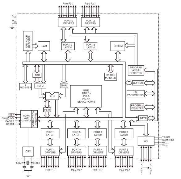
A simplified version of the Intel 87C51GB single-chip microcontroller architecture [14] is shown in this figure. All program memory address buses are 16 bits wide, but the internal RAM and SFR can be accessed by 8-bit addresses. Sixteen addresses in SFR are both byte and bit addressable. The upper two I/O ports (0 and 2) generate a 16-bit
address, where port 0 is multiplexed as an 8-bit data bus for instruction fetch. The program counter generates the programs addresses sequentially, and the 8-bit instruction words are fetched to the instruction register and then executed by the CPU. For an interrupt or jump instruction, the next address is stored in the stack pointer and the PC is vectored to the new address. The eight registers, PSW (program status word), stack pointer, DPTR (data page pointer to generate 16-bit external data address), and port latches shown are all part of the SFR (special function register). The successive approximation type A/D converter can be triggered externally or internally. AVss, AVREF, and COMREF (for comparison with sampled signal) are external analog voltages. The sampled signals are stored in the SFR. The ALU (arithmetic logic unit) processes the arithmetic and logic signals with the help of two temporary registers, and an accumulator (ACC) is the common destination for most arithmetic and logical operations. All five counters on the chip can be programmed for a variety of functions. The oscillator clock on the chip requires external crystals as shown. EPROM is good for initial program development, but PROM (mask programmable ROM) is economical for the final product.