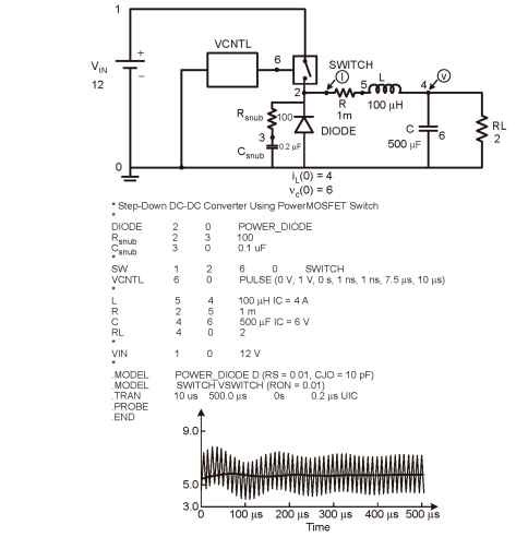
A very simple buck converter, as shown here, is considered for a simulation study [6]. All circuit components, along with the diode and power MOSFET models, are stored in a library. Once the circuit is designed, the schematic is drawn in a window by dragging in the elements and assigning their attributes in the dialog box. A schematic can be large and cover several pages. In this example, the diode is characterized by conduction resistance of 0.01 ohm and junction capacitance of 10 pF in open circuit. The switch conduction resistance is 0.01 ohm and open circuit resistance is infinity. The gate drive is defined by Stimulus Editor, or else the control circuit can be drawn in schematic form. In this example, a PWM wave of 1.0 V at 100 kHz with a duty ratio of 0.75 is defined. The resulting V (solid) and I (oscillatory) (as marked) waves are shown at the bottom of the figure. Instead of drawing the schematic, the user can create the file (netlist) as shown using the Text Editor. Numbering of nodes is not needed for schematic entry.