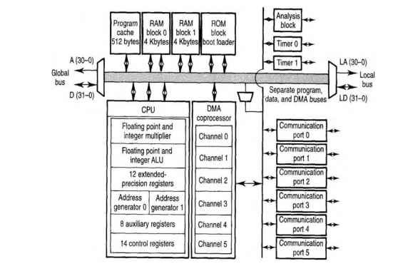
A simplified architecture for the C40 DSP is shown in the figure. The detailed architecture and description are given in Ref. [17]. Again, the fast instruction cycle time is possible because of the pipeline architecture (i.e., overlap of program fetch, decode, read, and execute operations). The DSP can be used in either microprocessor or microcomputer mode. In the latter mode, the ROM block boot loader becomes active. This on-chip code transfers program from an external memory or from a communication port to its RAM at power-up reset. The 512-byte (128-word) on-chip instruction cache is provided to store often-repeated sections of code, thus reducing the number of slower off-chip accesses. The 31-bit address bus and 32-bit data bus for local and global buses support large external memory space and help in parallel processing. The "analysis block" shown permits hardware and software debugging for a parallel processor system. Six identical communication ports permit bidirectional 8X32-bit FIFO (first-in-first-out) mode data transfers either under the control of the CPU or DMA coprocessor. The DSP can support a wide variety of multiprocessor architectures (such as rings, trees, hypercubes, bidirectional pipelines, two-dimensional Euclidean grids, hexagonal grids, and three-dimensional grids) to speed up complex system operations. The DMA coprocessor that supports six DMA data transfer channels (32-bit wide) operates in two basic modes: unified mode (memory-to-memory transfer) and split mode (two-way memory-to-communication port transfers). The DSP does not have any serial ports.